Introduction
In this lab, we explored the concept of system linearity through various experiments involving different modules. The objective was to understand the linearity of systems by evaluating their response to scaling and additive inputs. Using the TIMS equipment, the Voltage-Controlled Oscillator (VCO) was connected to different modules such as the comparator, rectifier, and multiplier, with the goal of determining whether these systems adhered to the principles of linearity. The experiment particularly focused on observing if the system output scaled linearly with increasing input voltage and whether it maintained additivity when different input signals were combined. These findings were analyzed using the PicoScope to record and interpret the output signals.
Procedure
Part A: Linearity and Scaling
Part A1: Comparator
Part A1 begins by preparing the VCO and UTILITIES modules on the TIMS rack. The VCO’s sinusoidal output is connected to the buffer amplifier input and a frequency counter. The buffer amplifier’s output is then connected to the UTILITIES module comparator input and to an oscilloscope channel. Using the Pico Scope, the VCO’s frequency is adjusted to around 1000 Hz, and the buffer amplifier gain is set to achieve a 1V peak-to-peak signal. The goal is to observe the system’s response and collect data for different input voltages.
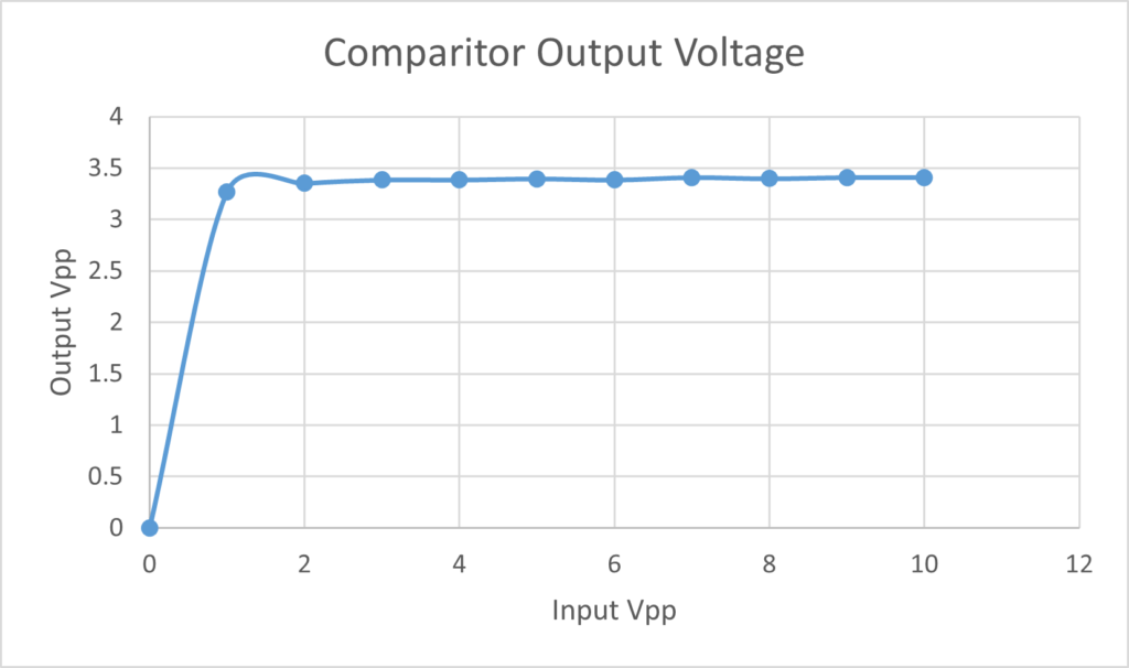
As we can see from Figure A1.1, the voltage out does not linearly change at all with a linear increase in output voltage. Instead see the output voltage jump to a steady level, around 3.3 volts after the input voltage surpasses 1 volt. This leads us to conclude that the comparator is not a linear system.
Part A2: Rectifier
In Part A2, the setup from A1 is modified to study the rectifier system instead of the comparator. The buffer amplifier’s output is connected to the rectifier input and an oscilloscope channel, while another channel is connected to the rectifier’s output. Using PicoScope, the input signal is adjusted to a 1V peak-to-peak sinusoid at 1000 Hz. The rectifier output is then observed, and the input signal amplitude is increased in 1V increments to record the peak-to-peak output values.
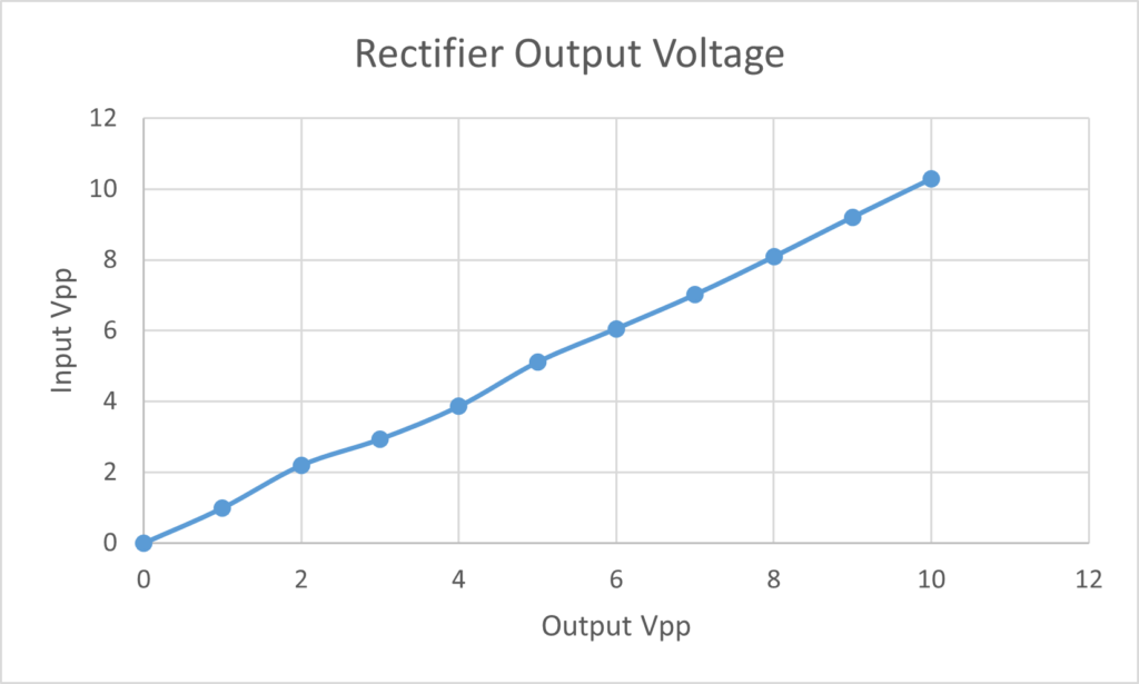
In this case, we see a linear increase of output voltage with an increase in input voltage. Figure A2.2 alone may lead us to believe that rectifiers are linear however this is misleading. Rectifiers only reflect the positive side of a voltage signal, meaning that any negative portion of a signal is lost, such as half the voltage in a typical AC signal. For this reason, rectifiers are not linear despite the linear behavior observed in our experimentation.
Part A3: Multiplier
In Part A3, the setup is prepared to study the multiplier system. First, the VCO is connected to the buffer amplifier and frequency counter, and the VCO frequency is set to 1 kHz. The buffer amplifier’s output is then connected to both inputs of the multiplier and to an oscilloscope channel. The multiplier’s output is connected to another oscilloscope channel. Using PicoScope, both channels are set to DC coupling, and the time base is adjusted to view multiple cycles. The buffer amplifier gain is adjusted to achieve a 1V peak-to-peak input signal, and the output amplitude is recorded. The results are used to assess the system’s linearity.
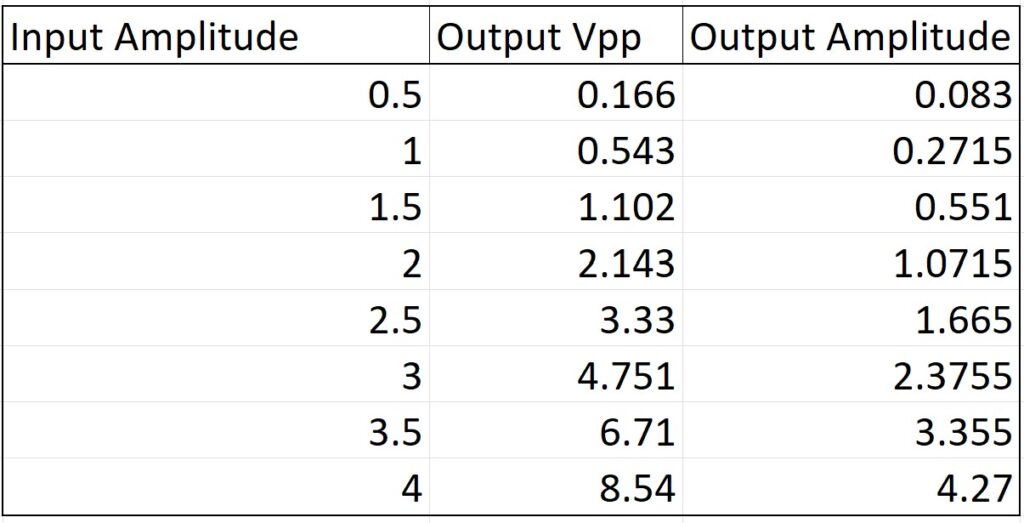
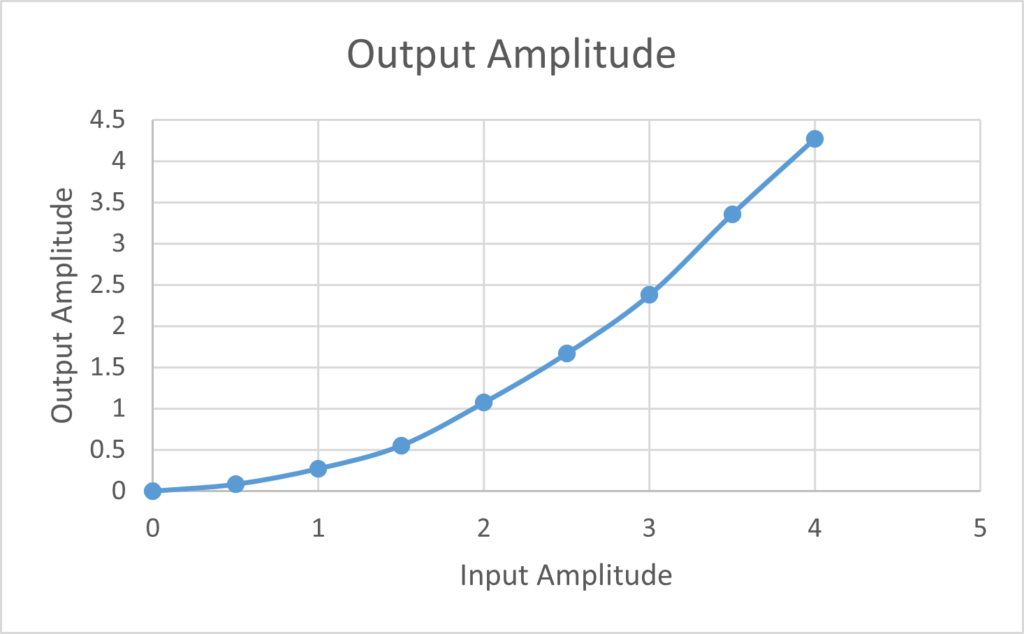
As we can see in Figure A3.1, the output amplitude as a result of the input amplitude increasing shows us something that resembles exponential growth more so than linear growth. This leads us to conclude that the system is not linear because it fails to uphold the scaling property.
Additionally, in the beginning of this section the half angle formula was used as a proof to show why a system that squares its input, such as a multiplier with the two inputs connected would not be linear. I think this proof can be applied to further confirm that multiplier system in question is not linear. We see from the output of the figure above that the system is likely simply squaring the input, which we have already proved in the lab manual to fail the scaling and additivity properties and therefore be nonlinear.
Part B: The VCO as a system
Part B1: DC Voltage Control
Steps 1 through 6 of Part B1 in the lab outline how to set up and observe the behavior of a DC-controlled Voltage-Controlled Oscillator (VCO). First, disconnect all leads and power off the PicoScope. Assemble the TIMS rack by ensuring the VCO is properly configured, with its switch set to “VCO” and toggles centered. Then, connect the VARIABLE DC output to both the VCO input and Scope ChB, while the VCO output goes to the FREQUENCY COUNTER and Scope ChA. After setting up the PicoScope with appropriate trigger and time settings, adjust the DC output to -2V, then record the corresponding frequency from the FREQUENCY COUNTER. Repeat this step for different DC output values, filling in a table to document the results
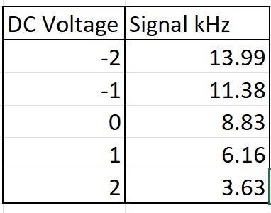
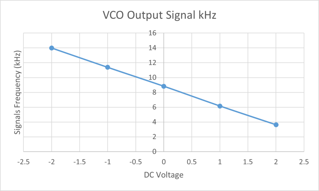
As we can see from the graph above, there is a linear decreasing relationship between the input DC voltage and the frequency of the VCO’s output signal. This leads to us to conclude that for the range we tested, the VCO is a linear system. While is true for our experiment, it is important to note that the linearity of a VCO breaks down when its inputs near the edges of its operating range which is why the VCO is not truly linear even though we deem it so for our purposes.
Part B2: Frequency Control
In Part B2, the steps focused on studying a frequency-controlled VCO. First, all leads were disconnected, and the PicoScope was turned off. The TIMS rack was then set up by inserting the AUDIO OSCILLATOR and VCO modules. The AUDIO OSCILLATOR’s sinusoidal output was connected to both the BUFFER AMPLIFIER input and the FREQUENCY COUNTER, and the AUDIO OSCILLATOR was adjusted to achieve 300 Hz. The BUFFER AMPLIFIER output was connected to the VCO’s input and to Scope ChB, while the VCO’s output was connected to Scope ChA. The PicoScope was configured with appropriate trigger settings and time base. It was then observed that the input signal modulated the VCO output frequency, with higher input values decreasing the output frequency and lower input values increasing it
Noticing how the input signal controls the frequency of the output signals oscillation and interesting application comes to mind. This could be used to control an AC motor. For example, since the frequency of the motor control controls the angular acceleration of the motor shaft, you could connect a VCO’s output to a motor and then change the value of the DC input signal to more easily control the speed of the motor in a linear fashion.
Part C: Feedback System
Part C1: The Integrator
In Part C1, we explored the operation of an integrator. First, we disconnected all the leads and turned off the PicoScope to start fresh. Then, we set up the TIMS rack by inserting the AUDIO OSCILLATOR, UTILITIES, and LAPLACE V2 modules. The AUDIO OSCILLATOR’s output was connected to the UTILITIES COMPARATOR input and the FREQUENCY COUNTER to achieve a 1 kHz signal. Next, the UTILITIES output was connected to the LAPLACE V2’s S1 input and to Scope ChB, and the S1 output was connected to Scope ChA. After configuring the PicoScope with DC coupling on both channels and adjusting the time base, we stabilized the scope output using the auto trigger to observe how the integrator worked.
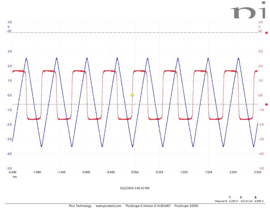
As we can see in Figure C1.1, when we input the square wave signal to the integrator, we find the output to be a triangular wave. Additionally, we see the peaks of the triangular wave signal line up with falling and leading edges of the square wave because that is when the slope is changing thus the value of the integral at the moment changes. This is exactly the behavior we would expect considering the integral of a square wave is a triangular wave.
Part C2: Feedback System
In Part C2, we applied what we learned about the integrator to a feedback system. First, we disconnected all the leads and turned off the PicoScope to start fresh again. We then inserted the LAPLACE V2 and TRIPLE ADDER modules into the TIMS rack for the feedback study. After that, we connected the ARB2 output to Scope ChA to check the signal, and we turned on the S&S V2 SFP application to load the ARB signal. Once the ARB2 signal was visible on the PicoScope, we set up the TRIPLE ADDER by selecting the correct slot position and adjusting the gains (b1 = 1, b2 = -1). We then assembled the feedback circuit by connecting the ARB2 output to the TRIPLE ADDER input and wiring the TRIPLE ADDER and LAPLACE V2 modules as shown in the block diagram. Finally, we adjusted the PicoScope settings to capture the input and output signals and observed how the system responded, with the output showing an exponential decay, which we used to measure the time constant.
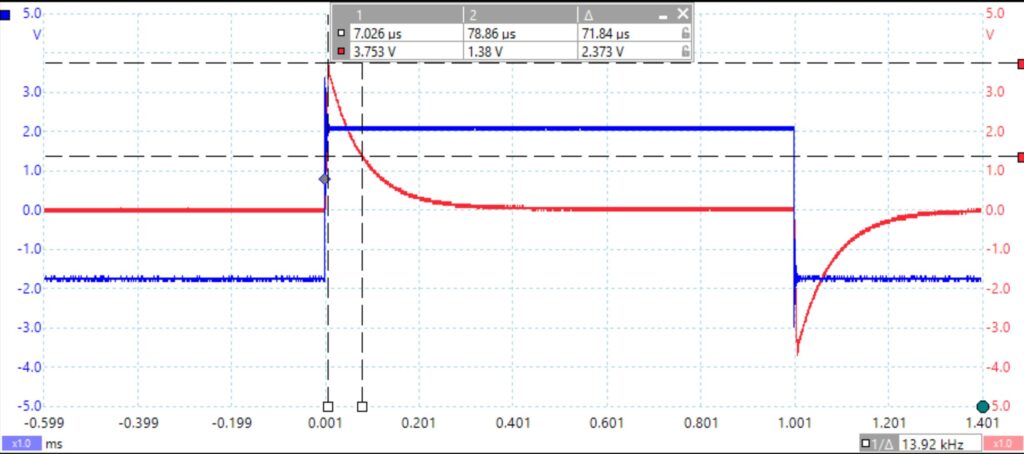
As we can in the above the figure, using the cursors we measure the time constant by comparing the difference between the top value and when the signal has reached e^-1 of its top value. The time constant was found to be 71.84uS.
Conclution
This lab was a great way to apply the theoretical concepts of system linearity and feedback that we’ve been learning in class to real-world systems. I especially liked how we got to physically see how things like voltage-controlled oscillators (VCOs), comparators, rectifiers, and integrators behave, which really helped solidify the ideas of linearity, scaling, and feedback. It was satisfying to observe the direct relationship between the input signals and the resulting system outputs, making the abstract concepts from class much more tangible. Overall, I found the lab to be both informative and engaging, and there wasn’t anything I didn’t enjoy about it. It was a well-rounded experience that tied in the classroom material in a hands-on way, which I really appreciated.
Leave a Reply