Introduction
The purpose of this lab is to explore the concept of convolution and its practical applications in hardware systems. By reconstructing and analyzing a system’s response to various inputs, students will deepen their understanding of key principles such as superposition and the unit pulse response. The experiments build on foundational knowledge from previous labs, using the TIMS hardware platform to demonstrate the convolution process and its relationship to linear time-invariant (LTI) systems. Through hands-on configuration and observation, students will examine how input signals, including discrete pulses and a rectified sine wave, interact with the system to produce output signals. These exercises aim to reinforce theoretical concepts while developing practical skills in signal analysis and system characterization.
Procedures
Unit Pulse Response
Below, we can see the initial setup used for the experiment in both a system diagram and a wiring diagram detailing how we created this system using the TIMS workbench. As you can, essentially, we set up a clock signal at 1 kHz using the 8.3 kHz reference clock provided as well as dividers in the digital utilities’ module. That signal is then passed to three different inputs of an adder. The second adder input is simply the first with a unit delay, and third input is the second with another unit delay applied. Additionally, the adder had its gain settings changed. The first input was set to 0.3, the second to 0.5, and the third to -0.2. This essentially is the multiplier applied to the signal before it is included in the adder. In the wiring diagram, the adder module obviously acts as the adder and the inverse Z transform modules were used to give us the unit delays. The diagrams describing this can be seen below.
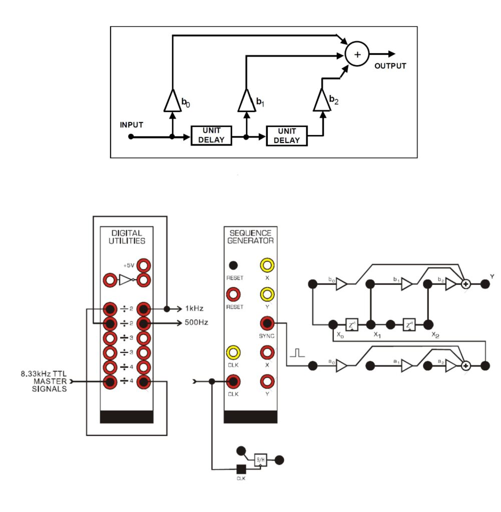
When we observe the unit pulse response generated by the input, we see that is it is three consecutive pulses that match up to gain settings applied to the adder. These come one after the other and do not interfere with each other because of the delays applied to the signal. In the physical world, a time-delay in a signal can be introduced by the use of a capacitor, which can store the energy in a signal and then release it later in time.
The Superposition Sum
The lab manual explains the concept of discrete convolution and its application in Linear Time-Invariant (LTI) systems. The equation for discrete convolution describes the relationship between the input signal and the impulse response of the system. It is expressed as the sum of the product of the input signal values and the shifted and flipped impulse response. For LTI systems, the output is determined by the convolution of the input signal with the system’s impulse response. This means the output is a combination of scaled and shifted impulse responses, where the input values act as weights that determine how much each shifted response contributes to the overall output.
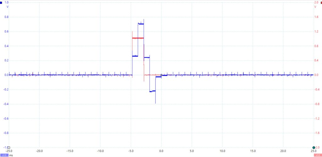
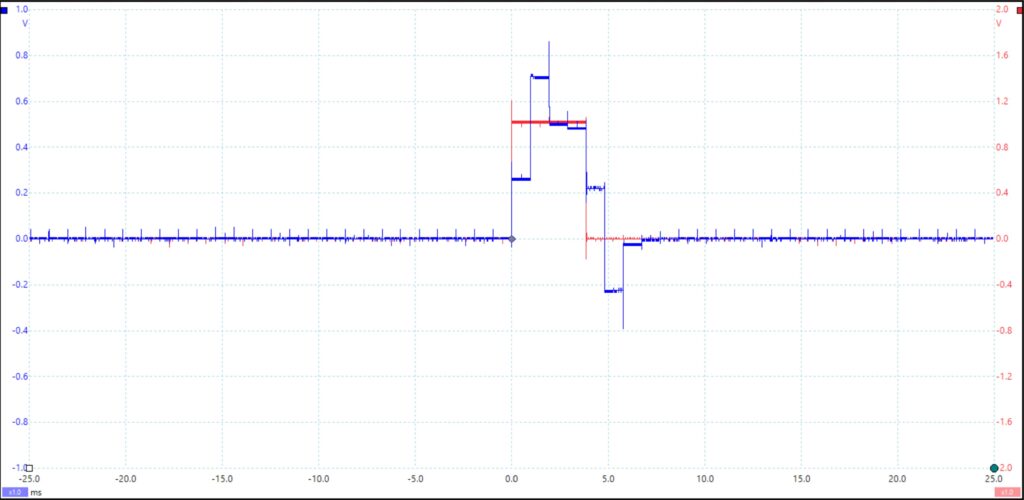
As explained earlier, convolution involves summing up the scaled input responses of the system. When the clock frequency is reduced from 1000 Hz to 500 Hz, the sync pulse width doubles. This change causes the system’s output to shift from three levels to four, which is different from the behavior observed in Lab 8. If the input were extended to four pulses further dividing the clock in half again, the output would theoretically increase to five pulses. Achieving this would require adding more delay modules to the chain and including an additional adder module for the new delays.
Rectified Sine Wave As Input
The TIMS unit is then set up as shown below. The input for the system is rectified sine wave shown in the diagram below. Each output (b0-b2) is recorded individually, along with the final output. The error in y[2] was calculated as 1.9 – 0.532 + 1.55 – 0.89 = -0.708 V. For y[0], the error was 0.97 – 0.741 + 0.76 – 0.1 = -0.431 V, and for y[1], the error was 2.17 – 0.925 + 1.08 – 0.35 = 0.515 V. The equations for the outputs are as follows and the resulting signals are illustrated below as well.:
- y[1] = (0.3)x[1] + (0.5)x[0] + (-0.2)x[-1]
- y[2] = (0.3)x[2] + (0.5)x[1] + (-0.2)x[0]
- y[6] = (0.3)x[6] + (0.5)x[5] + (-0.2)x[4]
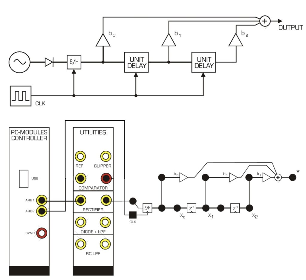
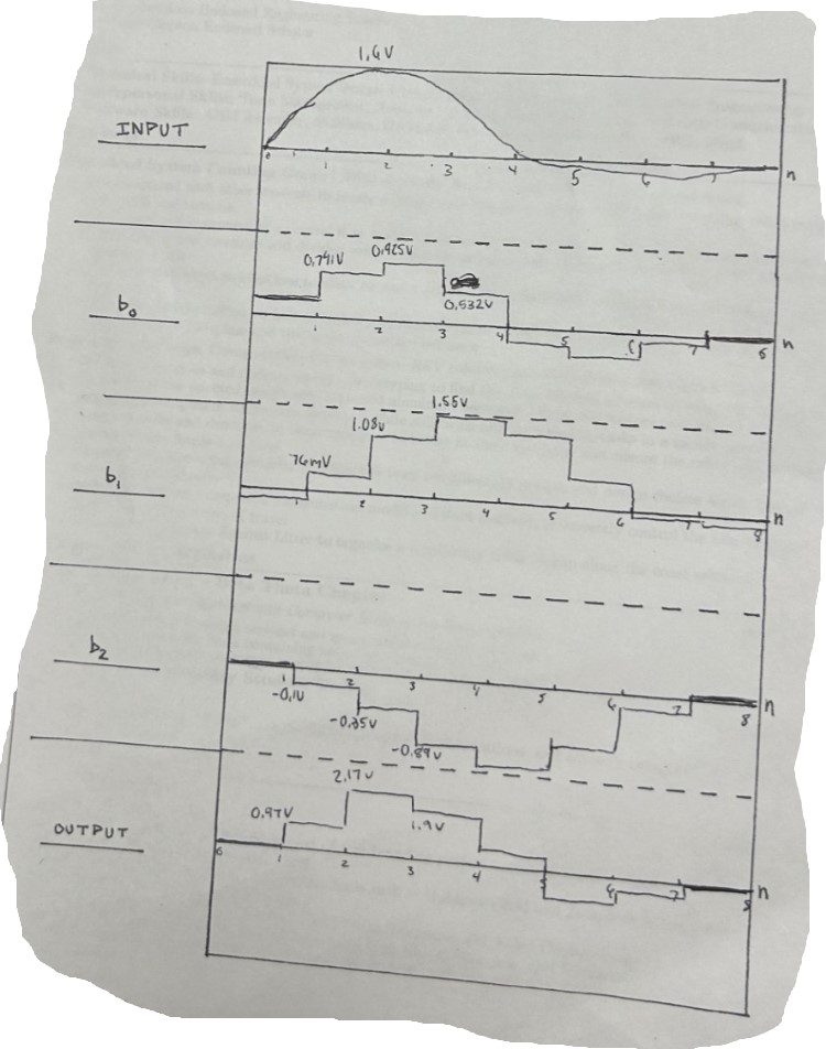
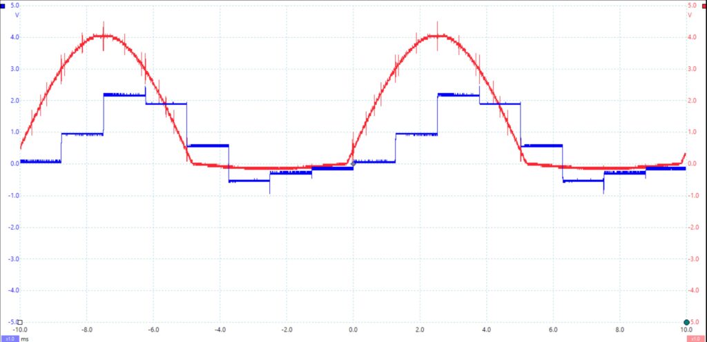
While there was certainly some error present, an average of about 0.6 V, we can still amount that to poor connections and things outside of our control because the error does not ever exceed or come very close to 1 V. Additionally, the input rectified sine wave along with output of the constructed system can be seen below.
Conclution
In conclusion, this lab successfully demonstrated the practical application of convolution in hardware systems using the TIMS platform. By analyzing the system’s response to various input signals, including discrete pulses and a rectified sine wave, the relationship between input-output behavior and the principles of superposition and the unit pulse response was clearly observed. The step-by-step configuration and verification of system components reinforced theoretical concepts such as the convolution sum and its role in linear time-invariant systems. Overall, this experiment provided valuable insights into how signal processing concepts translate into real-world hardware implementations, bridging the gap between theory and practice.
Leave a Reply