Introduction
This experiment focuses on exploring the convolution process in discrete-time systems through practical application. Convolution, typically introduced as a mathematical formula, is approached here via hands-on experience to reveal its fundamental principles. By observing basic signal inputs within a linear system and measuring the resulting outputs, this lab allows us to visualize convolution as a running average of successive input values. Key aspects include understanding the system’s unit pulse response and superposition properties, with a special emphasis on sine wave behavior in time-domain filters. Through this approach, we aim to demystify convolution as it applies to real-world signals and filtering systems, providing foundational insights into its practical and theoretical applications.
Procedure
Part 1
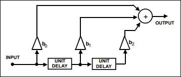
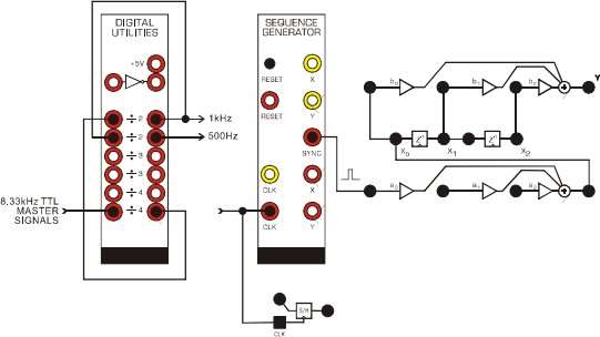
In part one, we began by setting up the experiment. First, we connected the PC modules controller to the lab computer in order to make use of arbitrary signals in our lab activity. Next, we started the companion software and loaded up the relevant lab. The digital utilities module was then used to create a 1kHz and 500Hz sample clock for use throughout the lab and the circuit shown in the block diagram and wiring diagram below were constructed.
Next, we measured the input clock signal to ensure that it is what we expected as this signal is an important component of the systems we were tasked to construct. The PicoScope graph can be seen below.
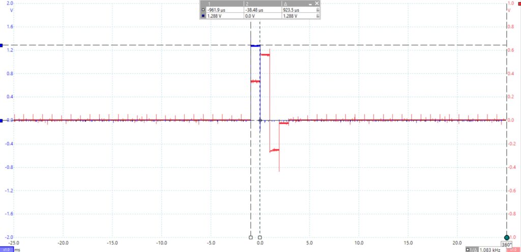
The signal in question here is the blue signal from channel A. This is the clock input signal, as we can the pulse lasts for about 1 ms, which further confirms that is it a 1 kHz clock. Additionally, the pulse has an amplitude of about one 1.25 V. We notice that we see the input pulse once every 32 periods. This is because of the manor in which signal is created using the multiple division blocked provided in the digital utilities module.
Part 2
In Part 2 of the lab, the focus is on examining the unit pulse response of a delay line system to understand how an isolated input pulse is processed in a linear time-invariant system. The delay line is configured with three adjustable tap gains: b0 = 0.3, b1 = 0.5, and b2 = -0.2. A single pulse is used as the input, and its propagation through the system generates delayed and scaled replicas. The output, observed using an oscilloscope, consists of three contiguous pulses whose amplitudes directly correspond to the values of the tap gains (b0, b1, b2). This demonstrates that the output is a superposition of scaled and delayed versions of the input pulse, aligning with the theoretical definition of the unit pulse response h(n), where h[0] = b0, h[1] = b1, and h[2] = b2. The experiment also highlights practical energy storage effects in real systems, such as inertia in mechanical systems and reactive components like capacitors and inductors in electrical circuits. This foundational understanding of the unit pulse response sets the stage for exploring convolution in more complex input scenarios in later parts of the lab.
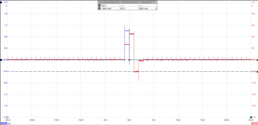
Additionally, the amplitude of each pulse in the output was measured and recorded in the table below.
| Pulse | Amplitude (mV) |
| h[0] | 273.2 |
| h[1] | 456.1 |
| h[2] | -204.3 |
Part 3
In Part 3 of the lab, the concept of superposition is explored by observing the system’s response to two consecutive pulses as input. The sequence generator’s clock rate is halved to create a longer pulse width, resulting in two contiguous pulses. Using the same gain settings as in Part 2 (b0 = 0.3, b1 = 0.5, b2 = -0.2), the output signal is observed to consist of four nonzero pulses per frame. The amplitudes of these pulses demonstrate that the output sequence is the sum of two offset unit pulse responses. By plotting and superimposing the graphs of the individual responses, it is shown that the resulting output is a linear combination of these shifted responses, confirming the principle of superposition in linear time-invariant systems. This experiment highlights how a series of summed impulse responses can represent the system’s behavior for more complex input sequences, forming the basis for understanding convolution as a mathematical operation in signal processing.
Below, you can find the graph of the signal from part two, the signal from part two delayed one-time unit, and the superposition of the signals as experimentally seen in part three.
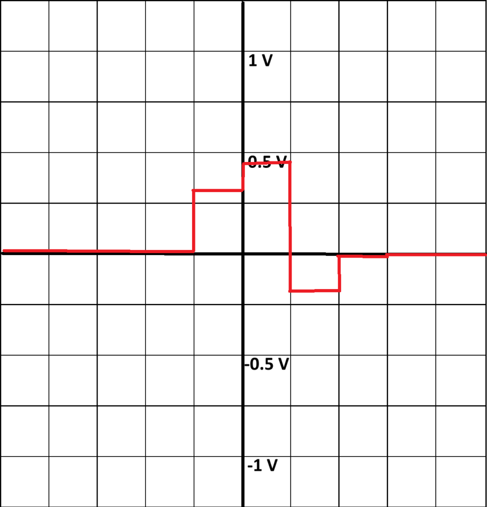
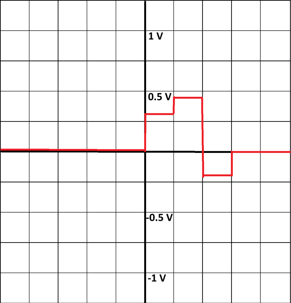
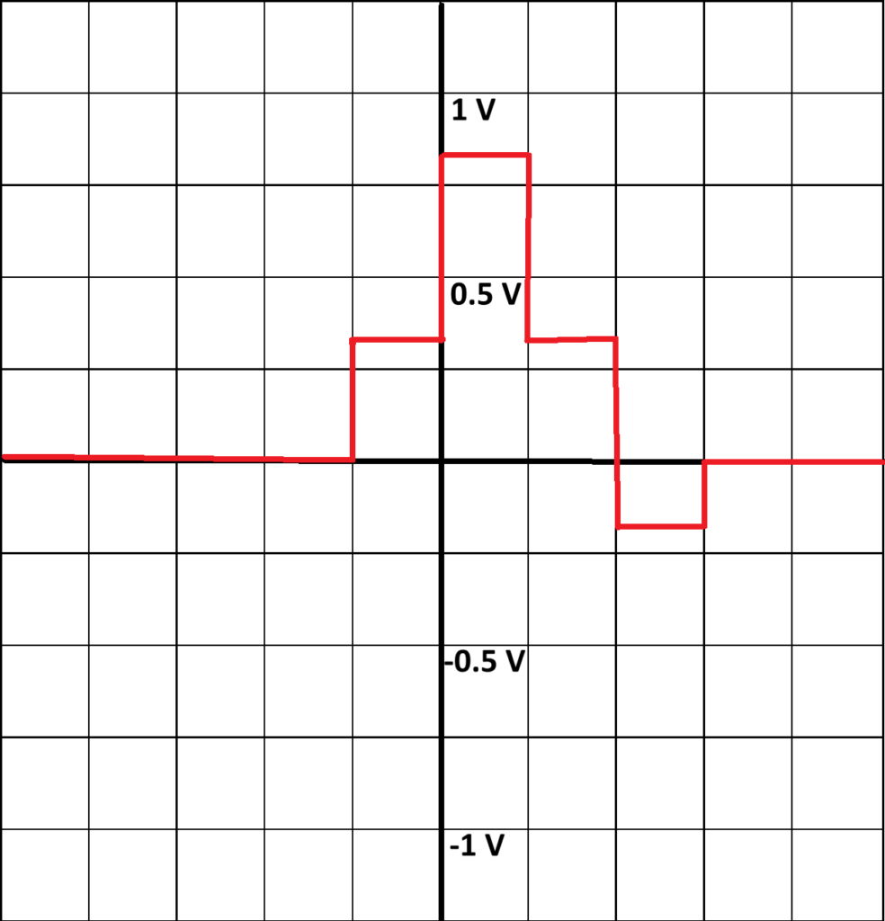
In the companion software, the gains for the adder inputs are set to b0 = 0.3, b1 = 0.5, and b2 = -0.2. The scope inputs are adjusted to measure the delay line input signal and the adder output signal. The resulting waveform is shown in Figure 3. The amplitudes of the pulses in the output sequence are measured, with h[0] recorded as 0.273 V, h[1] as 0.456 V, and h[2] as -0.204 V.
Part 4
In Part 4 of the lab, a more complex input is introduced by using a half-rectified sinewave to analyze the system’s behavior. The sinewave, generated by ARB1 at 100 Hz with a peak amplitude of 2 V, is rectified and then sampled by the SAMPLE/HOLD block at a clock frequency of 800 Hz from ARB2. This sampling process converts the continuous rectified sinewave into a sequence of discrete pulses while maintaining synchronization with the system clock. The input and output signals are observed, showing eight samples per half wave of the rectified sinewave. Using the same gain values as before (b0 = 0.3, b1 = 0.5, b2 = -0.2), the system’s output is analyzed to demonstrate how the sampled input signal is transformed by the delay line and gain settings. The experiment emphasizes the role of the SAMPLE/HOLD block in discretizing the input signal without digitizing it, a distinction crucial for understanding signal sampling. Additionally, this exercise builds on previous insights into the linear and time-invariant nature of the system by extending the analysis to a non-impulse, continuous input signal.
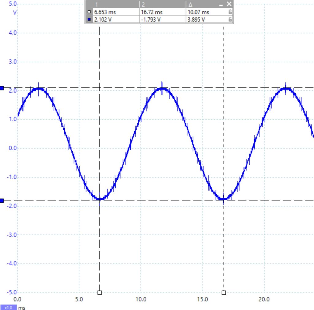
As you can see from the oscilloscope output above, the ARB 1 input waveform has a peak to peak voltage of 3.895 V and a period of 10.07 ms. When the corresponding calculations are performed, we see that these measurements agree with the desired signal with an amplitude of 2 V and frequency of 100 Hz.
Next, this signal was rectified and then fed to the S&H unit. The rectifier output and the S&H output can be seen below.
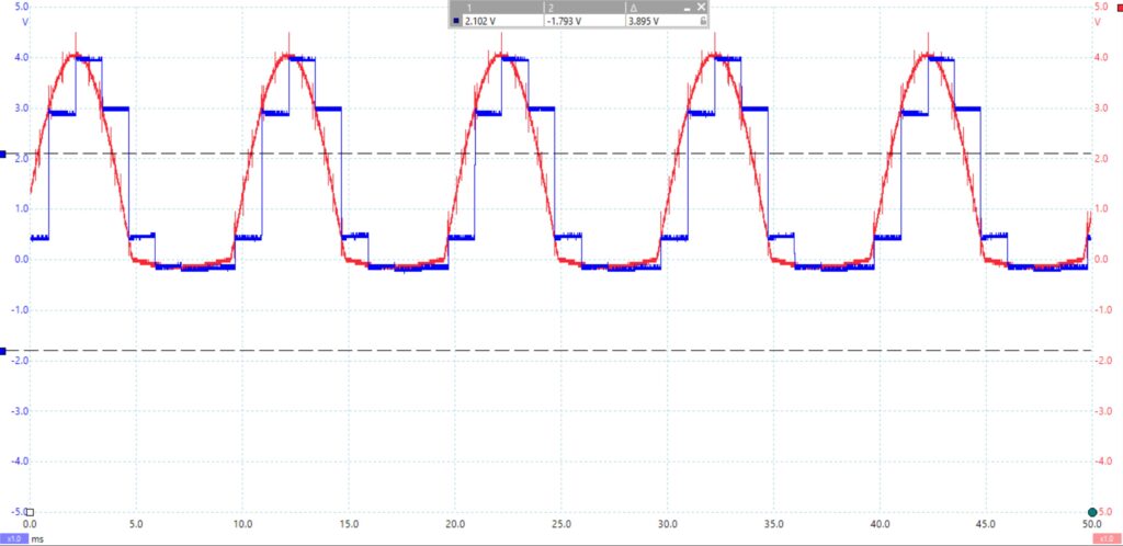
As you can see, the rectifier output is similar ARB 1 sinusoidal signal, except for the key difference that it has been rectified. This means that thru the use of a diode network the negative part of the signal has been removed, and in this case replace with essentially nothing or zero volts because a half sine rectifier was used.
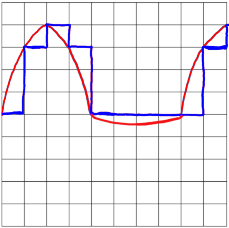
As we can see from our analysis of the input and output of the S&H system, it seems to function as a sort of analog to digital converter in the sense that it samples a continuous signal and outputs the sampled value, repeating this process at a regular frequency. That is, it samples the input signal at regular intervals and outputs the last sample taken until the next sample is measured. This is why is it called an S&H module, standing for sample and hold.
Conclusion
In conclusion, the lab demonstrates how a linear time-invariant system processes various inputs, from isolated pulses to more complex signals like a rectified sinewave. Through analyzing unit pulse responses, superposition, and sampled signals, the experiments highlight the principles of convolution and the system’s ability to transform inputs based on delay and gain settings. This foundational understanding is essential for applying convolution in signal processing and system analysis.
Leave a Reply