Introduction
In this lab activity, we used the TIMS unit to explore the properties of different signals as the they pass through systems. To do this we completed five different experiments and analyzed the results. These experiments studied digital pulse sequence, step input, impulse, sinusoidal signals, and digital detectors. Overall, this lab provided a physical aspect to the material covered in lecture that helps contribute to developing a complete intuition for this fundamental concept of electrical engineering.
Procedures
Part A – Digital Pulse Sequence
A1 – The Audio Oscillator
The audio oscillator is a TIMS module that provides a tunable sin wave output ranging from 300 Hz to 10 kHz, aka the audio frequency range. In addition to the sinusoidal signal, the module also produces a digital square wave with the same frequency called the TTL output. The TIMS unit has a built-in module called the frequency counter that counts the frequency of a signal it takes as an input. In steps one through five, we connected the TTL output to the frequency counter as well as the Picoscope to get a measurement of both the frequency of the signal and the voltage of the signal as a function of time. We then set the frequency of the audio oscillator 1 kHz using the adjustment knob then used the Picoscope to measure one pulse width and clock cycle. We found the pulse width to be 511.8 us and the clock cycle to be 976.3 us long.
A2 – The Sequence Generator
The sequence generator is a TIMS module that outputs two independent pseudorandom sequences called X and Y based off of a common external clock signal. These sequences can be sampled directly or as a TTL signal. For this experiment, we connected the audio oscillators clock signal to the sequence generators input and then compared the TTL form of the X sequence to the audio oscillator signal used to create it.
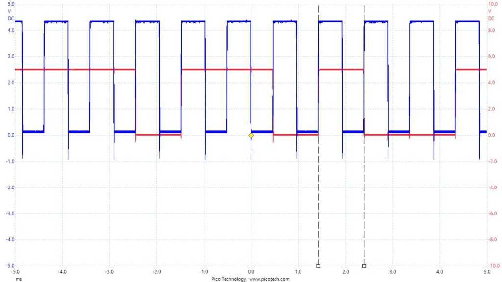
As we can see above in figure A2.1, the minimum interval between consecutive transitions of the digital signal is equal to two pulse widths or one clock cycle, measured between the cursor lines in the graph above as 977.1 us. While this value does not exactly match the measurement of the clock cycle duration, it is still safe to conclude that the minimum interval of the digital signal is equal to the clock cycle length of the sequence generators input. Using the rising edge of the clock shown in blue above to denote the beginning of the next bit, we can decode the signal and find the string binary 1101101001. We measured this pseudorandom string by examining the voltage of the red signal at the start of each blue clock pulse, beginning at the first rising edge on the left and ending on the last towards the right.
A3 – Baseband Channel Filters
The baseband channel filters module takes an input signal and passes it through one of three baseband low pass filters or a simple passthrough (no filter) based on the position of a knob. For this experiment, the filters serve as a source of response time limitation, and we will compare signals before and after they pass through the filter to examine this phenomenon. We began by connecting the 1 kHz output of the audio oscillator to the sequence generator and the oscilloscope. Then the TTL output of the sequence generator was connected to oscilloscope as well and the two were compared. The Picoscope was set to use 1ms/div time scale and AC coupling for both channels and the rise time, fall time, and delay and transition times caused by each of the three filters was recorded in the table below.
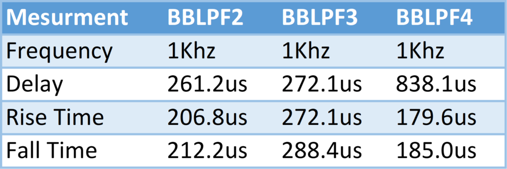
As per the lab procedure, we defined delay as the time between the clocks rising edge and when the signal voltage reaches 10% of the clock’s high voltage level. Additionally, we defined the rise time to be time it takes for the signal voltage to rise from 10% of the high value to 90% of the high value, and subsequently the fall time as the time it takes for the signal to reach 10% of the high value beginning when it crosses the 90% percent threshold.
Next, we explored effect of the input signals frequency on the output of the baseband filter, specifically BBLPF4. To do this, we slowly increased the frequency of the audio oscillator signal to 2 kHz and then until the bitstream of the sequence generator was no longer distinguishable after passing through the filter which we found to be at 3 kHz. Oscilloscope readings comparing the random sequence to the filters output can be found below for one, two, and three kHz.
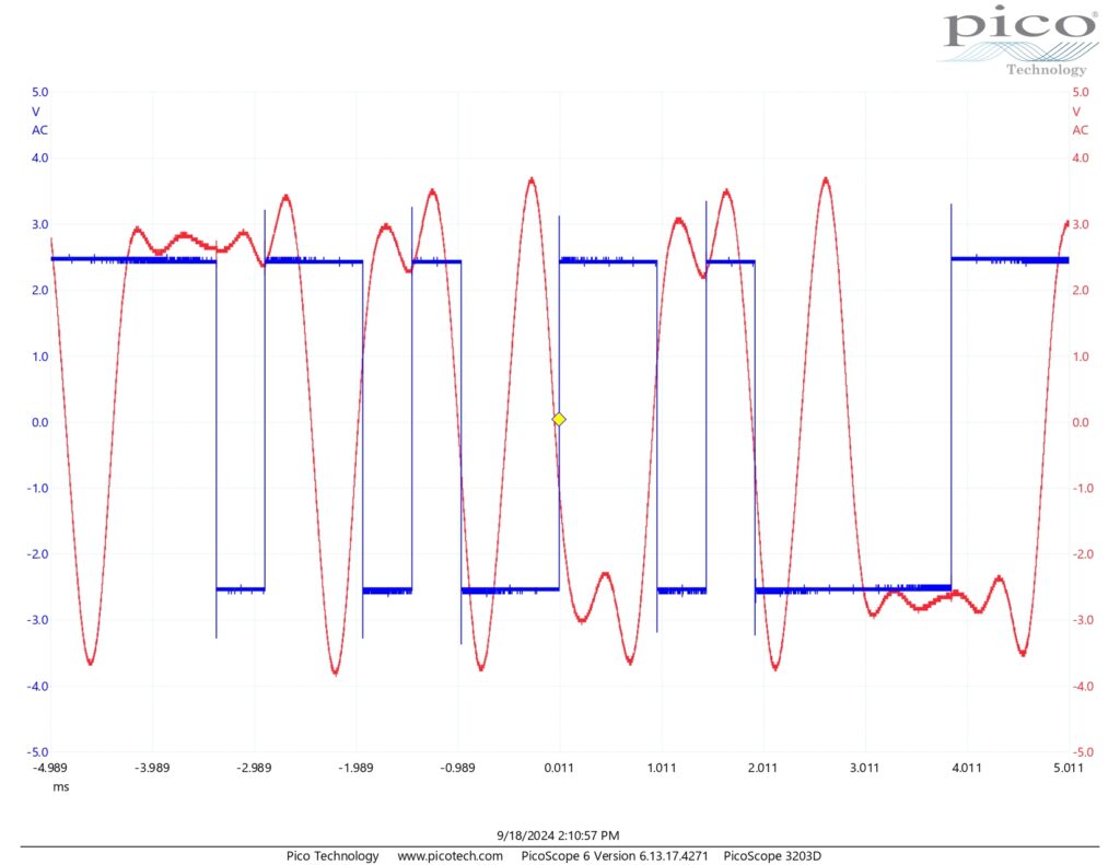
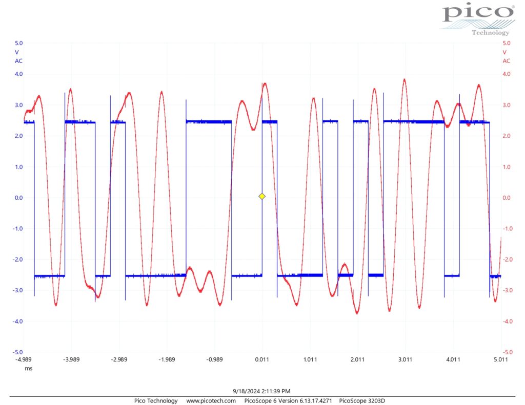
As we can see above, increasing frequency also increases delay. However, this is not the only factor contributing to the reduced ability to decode the sequence. Notice how the graphs above are scales identically yet figure A3.2 seems more horizontally compacted than figure A3.1. This is because increasing the frequency also increases the amount of information given per unit time which further contributes the degrading effects of the delay. I found at 3 kHz and beyond, it is no longer possible to accurately decode a bitstream from the filters output signal due to the significant effects of the filter.
Part B – Step Input
One method we can use to examine and characterize system delay and response is by examining its effect on a step function input. For this exercise we will employ this approach by examining the response to a long pulse. We began by connecting the TTL output of the audio oscillator to the baseband channel filters module’s input, and then comparing this input to the output with the Picoscope. We set the frequency of the audio oscillator to 0.25 kHz and then recorded the delay and rise times for each of the three filters given the same input signal as seen below in table B.1. One effect we noticed from the filter was ringing, when the response takes a certain amount of time to stop oscillating around the high voltage level and settle at it.

Part C – Impulse
In this section of the lab, we explored impulse and a given systems response to an impulse. Doing this with the TIMS systems comes with some limitations. For example, we are limited in the voltage of the pulse or the height, because we cannot produce infinite voltage. Given this caveat, for our experiment, the impulse will be a very short rectangular pulse with a voltage peak level that is reasonably obtainable with the TIMS. We began by connecting the audio oscillator’s TTL output (set to 0.25 kHz) to the corresponding sequence generator input, and the sequence generators sync output to the Picoscope using DC coupling. We then slowly increased the frequency and recorded the corresponding pulse width below in table C.1 before graphing the data in figure C.1.
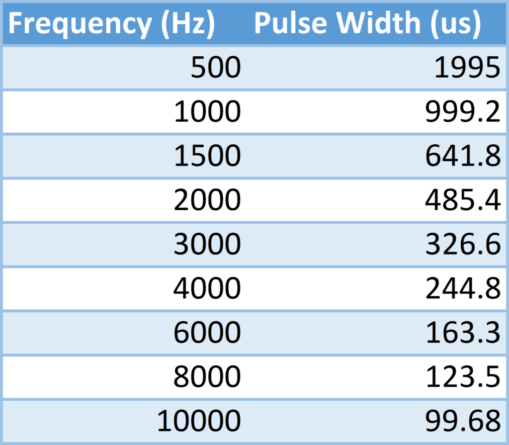
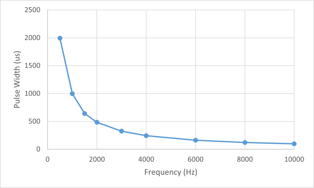
As we can see in the graph above, as frequency increases the pulse width decays exponentially. Next, we connected the sequence generators sync out which was measured above to the baseband channel filters module and then the output to the Picoscope. The audio oscillator was set to 300 Hz and slowly increased to 1000 Hz while observing the effect of this on the impulse response. We observed that as the pulse width got shorter as frequency increased, the rising edge of the impulse response gets closer to the falling edge of the impulse. Additionally, as the impulse width decreases the flat or stable region of the impulse response becomes shorter until it ultimately disappears. As we continued to increase the frequency to 2000 Hz the pulse width continued to shorten and the impulse response delay grew as its rising edge surpassed the falling edge of the impulse. Lastly, we observed the behavior as the frequency was increased to 10000 Hz. At this point now that the flat region of the response has disappeared, the shape remains the same while the amplitude decreases. This is because as we shorten the impulse width while leaving its amplitude constant, its energy represented by its area also decreases so the impulse produces a response with less energy. If we wanted the amplitude of the response to remain the same, we would have to increase the voltage of the impulse proportionally as we decrease the width.
Part D – Sinusoidal Signals
D1 – Basic Sine Waves
For this experiment, we connected the audio oscillator’s sin output to the buffer amplifier input and the output was connected the oscilloscope, frequency counter, and baseband channel filters module input. The audio oscillator was set to 300 Hz, BBLPF2 was selected, and the output was recorded on channel B of the Picoscope. The Picoscope was then used the adjust the buffer amplifier until a signal of six volts peak to peak was achieved. Then, for each of the three filters, the frequency of the input signal was adjusted while maintain six volts peak to peak and the resulting output signal’s peak to peak voltage was recorded below in table D1.1.
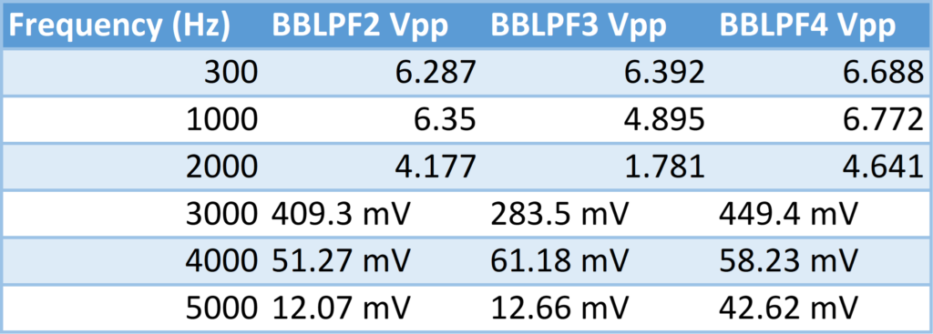
As we can see, despite some values that stand out as possibly erroneous due to human error, there is still an evident trend. As frequency increases peak to peak voltage decreases. The level of decrease is dependent on the filter however they all decrease. Additionally, as frequency increases, the output signal becomes fuzzier or has more noise, which proved to be challenging to accurately measure.
D2 – Clipping
In this portion of the lab, we used the utilities module to examine how the clipper utility can turn as sine wave into a square wave. The audio oscillator’s sine output was set at 1 kHz and connected to the buffer amplifier. The output was then connected to the utilities module’s analog signal input and the Picoscope along with the clippers output. The buffer amplifier was then adjusted from six volts peak to peak to achieve a input signal to the clipper of 300 to 350 mV peak to peak. As this adjustment took place, the input signal became noticeably noisier and the output signal began to resemble a sine wave more than a square wave. This is because the input signals voltage became too low to effectively and reliably trigger the clipper, so a square wave was not formed. Next, the input signal was adjusted to 20 volts peak to peak. This resulted in a clear, noiseless, input signal and an output signal that much more closely resembles a square wave. This the higher peak to peak voltage triggers the clipper more reliably due to the voltage being within the correct range as opposed to before.
Part E – Digital Detector
Any given digital signal will experience degradation when passing through a system. This does not necessarily mean that the signal is lost thought, if the degradation is not too severe the original signal can be recovered with the help of a digital detector. This is a crucial advantage of digital systems and what this section of the lab will focus on.
The audio oscillator’s sine output was connected to the sequence generator and the frequency counter. Then, the sequence generator’s audio output was connected to the baseband channel filters module as well as the Picoscope, and the output of the filter was connected to the Picoscope as well. This lets us observe the degraded digital signal that our clipper will attempt to recover versus the original. The output signal shows degradation similar to that seen earlier in this lab when a digital signal is applied to the filter. Next, we reconnect the Picoscope so that we could compare the digital signal to the clippers output. While the digital signal is still recovered, it has a delay now and is inverted. Next we increased that frequency, thus increasing the degradation by the filter, and eventually leading to errors when the signal is recovered by the clipper. This can be seen below in table E.1 where we compare the input and output bitstreams as the frequency is increased.

As you can see from the table above, it becomes increasingly more difficult to decipher a digital signal as its frequency rises and it degrades. We have an increasingly large delay that proves challenging to deal with when decoding the bit stream. Additionally, the output signal is inverted however this can be easily fixed by inverting the Picoscope channel when decoding the bitstream.
Conclution
Overall, this lab seemed to be one of the first challenging activities of this semester. Not only was it a race to finish on time in the laboratory, but it also combined five different concepts into one activity that made it seem rushed and overpacked. While these are all important to cover in this course, I think they could have been combined into more activities or spread out across other labs to create a better learning experience. Overall, I learned a lot from this lab, but it was relatively difficult and time consuming.
Leave a Reply